検索結果 Always_together
Always_together コミュニティ
1つのキーワードが1つのコミュニティです。
アカウント
見つかりません
Always_together を含む検索結果

📻 #ニッポン放送# ポッドキャスト
『Anime English Club with Sally Amaki』
エピソード67が配信されました🔥📣
ㅤ
🎧
🎥
今回の作品は、『サマーウォーズ』🗣️
家族同士、手を離さぬように。人生に負けないように。
もし、辛い時や苦しい時があっても、いつもと変わらず家族みんなそろって、ご飯を食べること。
いちばんいけないのは、お腹がすいていることと、1人でいることだから....
(栄)
Remember, never let go of fellow family members...
Never let life get the best of you...
And you always eat together as a family, even during difficult times...
Because being hungry and being all alone are the worst things that can happen to anyone...
(Sakae)
一緒に英語を勉強しましょう✨
@aec1242
#天城サリー# #SallyAEC# #ナナニジ#
もっと見る


チケット発売スタートしました😍
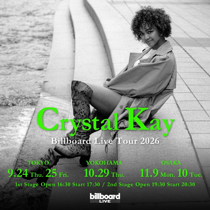
今年もビルボードライブツアーやります!東京、大阪そして久しぶりに横浜やるよ!みんなデート、お出かけ、観光プラスクリケイで楽しみに来てね♥️毎回みんなとその時にしか作れない空間がたまらないです😊今年もヤバスタルな時間にしましょう⭐
Ticket sales have started!
This year I'll be doing Tokyo, Osaka and Yokohama my hood! Its always a great intimate time at Billboard! Come down and lets have a great time together ❤️
Crystal Kay Billboard Live Tour 2026
1st ステージ (first stage)
開場 doors open 16:30
開演 show starts 17:30
2nd ステージ (second stage)
開場 doors open 19:30
開演 show starts 20:30
もっと見る

おはにゃん🐱💖
4月スタートだね、いつもそばにいてくれてありがとにゃ✨️
新しい月も、たくさん一緒に過ごせたら嬉しいな😊
これからも仲良くしてくれる?🩷
Good meowning 🐱💖
April has started, thank you for always staying by my side ✨️
I’d be happy if we can spend lots of time together this month 😊
Will you keep being close with me? 🩷
SFW illustration. No nudity or suggestive intent.
もっと見る


みんなー👋本日與真司郎は37歳になりました!!たくさんのお祝いコメントありがとう😭
ほんまに変わらずみんなから愛してもらえて僕は本当に幸せです🥹
そして、2026年4月22日、アーティスト活動を再開してから初となるフルアルバムのリリースが決定しました💙
約4年半ぶりのアルバムで、
アルバムのタイトルは「THIS IS HOW I AM」です🔥
日本語では、"これが俺の在り方”という意味で、今回のアルバムに入ってる全曲のプロデュース・作詞・作曲に参加し、等身大の與真司郎を作品に投影し、今僕が伝えたいメッセージがたくさん詰まっています🙈💙
詳細はオフィシャルサイトに随時更新していくのでチェックしてなっ😆
今年はこれからオンラインサロン旅行もあるし、トークショーもあるし、来年はアルバムをひっさげたフルライブツアーも💙
他にも動いてるものがあるからこれからも応援してくれると嬉しいです!!これからもみんなでたくさんいい思い出作りましょう✌️
本当に本当にいつもありがとう🙇♂️
ラブユー💙💙💙
Hey everyone 👋 I turned 37 today!! Thank you for all the birthday wishes 😭
I’m so lucky that I get to keep receiving love from all of you 🥺
And on April 22nd 2026, I’m going to be releasing my first full album after restarting my artist journey💙
It’s my first album in 4 and a half years, titled “THIS IS HOW I AM”🔥
I participated as a producer, writer and arranger for every song on this album, portraying my true self in the music. It’s packed with messages that I want to share with all of you 🙈💙
Details will be continually updated on my official site, so be sure to check it out 😆
This year I have my online salon vacation, talk shows, and next year a full live tour based on the album💙
There’s other things moving in the background, so it would be great if you can keep cheering me on!! Let’s keep on making amazing memories together✌️
Thank you always 🙇🏻♂️
Love you 💙💙💙
もっと見る


#ハネアメ誕生祭# #HaneAmeBirthday#
以前の私は、自分自身の成長のために努力していましたが、今はハネムン(Hanemoon fan)の皆さんと共に、歴史を作り上げるために奮闘しています。
今回、日本の秋葉原で開催されたバースデー展覧会は、私にとって非常に意義深いマイルストーンとなりました。これは、ただ数年間の創作の積み重ねにとどまらず、無数のハネムン(Hanemoon fans)の皆さんの支援の象徴でもあります。☺️
「展示会が素晴らしかった!」という皆さんの声を聞いたとき、これまでの努力がさらに意味深いものになったと感じました。長年にわたって私と協力してくださったLOVECACAO先生に、心から感謝の意を表します。また、会場でお祝いの花籠を贈ってくださったファンの皆さん、そして私を支えてくれた友人たちにも、深く感謝しています。
この数年間、MelonbooksやGoodSmile Companyからのご支援やご協力にも、心より感謝しています。
そして最後に、私が至らない点があった際にも、いつも寛大に見守り理解してくださったすべての方々に、心からお礼を申し上げます。本当にありがとうございました!🙇♀️❤️❤️
_______
In the past, my efforts were for my own progress; now, I strive forward to create history together with all the my Hanemoon fans.
The birthday exhibition held in Akihabara, Japan, was a truly significant milestone.
It represents not only the culmination of years of my creative work, but also the unwavering support of countless Hanemoon fans.
When I heard everyone say, "The exhibition was amazing!" it made everything even more meaningful.
I sincerely thank LOVECACAO, who has always worked with me,
as well as the fans who sent congratulatory flower arrangements at the venue, and my friends who helped me.☺️
Over the past few years, I am deeply grateful for the support and care from Melonbooks and GoodSmile Company.
Lastly, I want to express my heartfelt thanks to everyone who has shown patience and understanding during times when I have fallen short.
Thank you all so much!🙇♀️❤️❤️
もっと見る


Breaking down TSMC's glass core substrate slide
On June 11, at JPCA Show 2026 in Japan, TSMC gave a roughly 40-slide presentation titled "Advanced Packaging Technology Essential to the Evolution of AI" (AIの進化に不可欠な先端パッケージング技術). One slide from the deck, titled "Glass Substrate Development for CoWoS," has since leaked online and widespread attention.
Here's a closer read of that slide (see attached image). I'll skip the technical background that is already widely available. One thing to flag: the "COP" on the slide does not stand for Chip-on-Package. It means Coplanarity.
▌ Key conclusions:
1. TSMC has officially announced a partnership with Ibiden and Innolux to develop a glass core substrate. The structure is a three-layer design, a glass core sandwiched between two ABF build-up layers. This is the "oS" in CoPoS.
2. The market underestimates how important the glass core substrate is. It's a must-have capability for TSMC. In other words, within CoPoS the "oS" matters more than the "CoP", which is also why, when it was tested, it was paired with the existing CoW rather than with CoP.
3. The glass core substrate costs several times more per unit than existing ABF substrates. The glass processed by Innolux is very expensive per unit and is the single most critical material. Besides Nvidia, two US-based customers have also expressed strong interest.
▌ Industry checks tied to this slide:
1. The glass core substrate shown on the slide is cut from a full-size 250×250mm one. The ABF build-up layers mainly use Ajinomoto's GL107, mixed with ABF-GCP, and were tested at 24–28 layers, which is the mainstream ABF spec for AI chips in 2027–2028.
2. The CoW used in TSMC's experiment is a test vehicle. It is sufficient to validate the most challenging mechanical-structure issues that arise when working with composite materials. Good results mean TSMC, Ibiden, and Innolux have together broken through the critical technical bottleneck.
3. Ibiden currently handles cutting the 250×250mm glass core substrate. When the 510×515mm format is used for pre-mass-production simulation in 2H27, if Ibiden still wants to reduce production complexity to protect its ultra-high gross margins, it may hand the cutting over to Innolux, which is more familiar with the properties of glass.
▌ The leaked slide shows the validation results of pairing CoW with the "oS" in CoPoS, i.e., the glass core substrate (labeled "glass-SBT" on the slide). This addresses the "Substrate mechanical and electrical Dilemma" raised on the previous slide, and it strongly underscores how important the "oS" is within CoPoS.
1. Within CoPoS, what CoP solves is production efficiency / cutting economics, which ties to cost and price. What the oS solves is warpage and durability, which determines whether the chip can be made at all, and whether it can work.
2. CoP and oS complement each other well when integrated, but looking out over the next few years their technical roles still differ. CoP is a very-nice-to-have optimization, and going without it simply means a more expensive chip. But the oS is a must-have. Without it, even being able to make a usable chip is in doubt.
3. Comparing their roles isn't about elevating oS at the expense of CoP. It comes down to the practical question of which technical piece customers are willing to pay for. Details below.
▌ The real gold here is the power integrity (PI) improvement shown on the slide. This matters a great deal to customers, and it means that once glass core substrate production stabilizes, TSMC's profitability and competitive edge should rise in tandem.
1. How it works: the glass core substrate is thin → the vertical conduction path through TGV (through-glass vias) is short → conduction-path resistance (R) and loop inductance (L) both drop → PI improves.
2. Why it matters to customers: better PI → more stable power delivery → frees up power headroom → room to integrate more transistors, or to push clock speeds higher → more AI compute.
3. For customers, production efficiency is TSMC's basic responsibility, so they won't pay extra for it. But gains in AI compute translate directly into the customer's own competitiveness and profit, so customers are willing to pay for that. This is why Nvidia is so positive on the glass core substrate.
4. For TSMC, the glass core substrate raises yield and lowers cost while also boosting both the compute and the selling price of AI chips. It's both a cost-cutting tool and a pricing lever, a plus for profitability and competitiveness alike.
5. Substrate cost currently accounts for a low single-digit percentage of an AI chip's BOM, while losses from packaging yield run roughly 5–10× the substrate cost. So even if the glass core substrate ends up costing several times more than today's, its share of the BOM stays low, and it can cut the losses from packaging yield. The high unit price is therefore not expected to dampen customers' willingness to adopt it.
▌ In the Q&A after the presentation, an audience member asked about TGV details for the glass core substrate. TSMC declined to answer on the spot, because TGV is the key technology behind the glass core substrate, and the core know-how currently sits with TSMC and Innolux. By contrast, when another attendee asked about integrating IVR, eDTC, and LSI, TSMC answered at length.
▌ According to industry checks, if all goes well, TSMC is aiming to start mass production of the glass core substrate in 4Q28–1Q29, to match the cadence of Nvidia's AI chip iterations. As a side note: the Ibiden earnings presentation slide that many people have been circulating lists the glass core substrate timeline as CY30. My read is this: Ibiden, which has always been conservative and cautious in public, has now formally put the glass core substrate on its roadmap, which further confirms the long-term trend for this technology. That said, some other details on Ibiden's slide don't fully line up with what's known in the market. For example, its reticle timeline is off from TSMC's public claims by about a generation, and the Rubin Ultra substrate size is clearly larger than the 90×90 it marked for CY26–27. It's a reminder to always cross-check across multiple sources when forecasting the future.
もっと見る


「Always be here for you… always… 」
𝙏𝙝𝙚 𝙎𝙝𝙤𝙧𝙚𝙠𝙚𝙚𝙥𝙚𝙧 守岸人 - 鸣潮


AlwayS / NiziU 【現役アイドル】歌ってみた。
@YouTubeより