検索結果 stimulation
stimulation コミュニティ
1つのキーワードが1つのコミュニティです。
アカウント
見つかりません
stimulation を含む検索結果

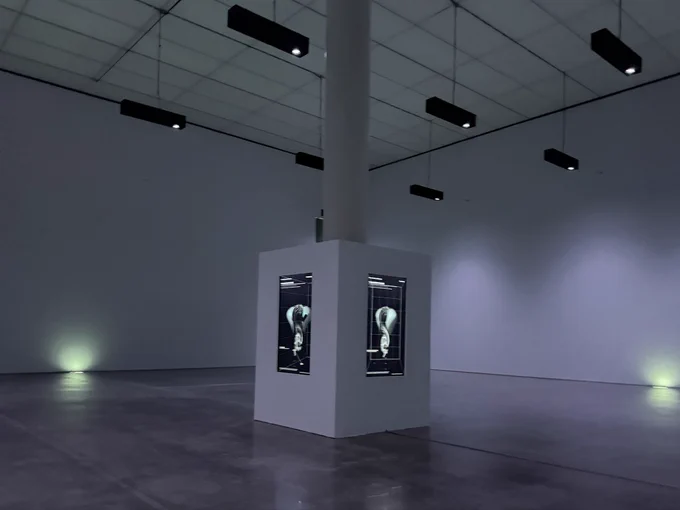
台湾・台中の臺中市立美術館で、真鍋大度の海外初となる大規模個展「RELATIONAL TIME — Life Beyond Simulation」が明日から開幕。
本展では、3つの新作を発表する。建築空間や身体感覚、リアルタイム・コンピューティング、映像、音、光を組み合わせ、観客の存在や動きに反応して変化する没入型の空間を生み出す。
もっと見る



A/Bテストって実施するだけで数週間かかりますよね。それ、実データ由来の「AIペルソナ」に事前予測させられるかもしれません。
タイトル: Data-Driven Persona-Conditioned Agents for A/B Test Simulation
URL:
❓ どんな質問の仕方がAIペルソナに一番効くの?
💡 バリアントを比較させる「ペアワイズ評価」が最も精度が高く、CTRで精度0.75、サブスクリプションで0.80を記録しました。単独評価だと0.40程度に落ちます。
❓ 実データがなくても代用できる?
💡 公開のe-コマースデータでもプロプライエタリデータに匹敵する精度が出ました。ただしドメインが違う映画レビューデータでは精度が下がり、ドメインの近さが重要だとわかりました。
❓ ペルソナは行動データが濃い方がいい?人口の多様性がある方がいい?
💡 CTR予測では行動データが濃い「深いプール」が有利でしたが、サブスクリプション予測では差が出ませんでした。目的次第で使い分けが必要そうです。
❓ ペルソナ数を減らすとコストは下がる?精度は落ちる?
💡 935人から500人へサブサンプリングしても精度はほぼ変わらず、約2倍のコスト削減に成功しています。
#A#/Bテスト #LLMエージェント#
もっと見る
🕶️ 自分の体の動きで一人称の世界を歩き回り、しかも「特定の場所に何があるか」を画像とポーズで指定して時間変化まで作れる——身体性のある一人称世界モデルAnchorWorldです。
タイトル: AnchorWorld: Embodied Egocentric World Simulation with View-based Evolution Customization
URL:
📝 概要
AnchorWorldは、人間の全身モーションで操作する一人称動画を生成する世界モデルです。さらに「アンカービュー」で、特定の3D位置に何が存在し、どう時間変化するかを明示的に指定できます。
❓ 解決する課題
既存の世界モデルは、一人称動画だけでは全身モーションの教師付けが難しく、環境も暗黙的にしか定義できませんでした。「自然な身体操作」と「局所的な世界カスタマイズ」の両方が欠けていたのです。
💡 方法論と提案手法
・一人称では体の多くが見えないため、三人称動画を補助教師に使い、全身と環境の位置関係を学習します
・アンカーはRGB画像・6-DoF視点ポーズ・進化プロンプトの3要素で、特定位置の見た目と時間変化を指定します
・3D RoPEで複数アンカーを空間的に区別し、masked cross-attentionでアンカーごとのテキスト制御を実現します
・三人称→一人称→静的アンカー→動的進化、の4段階で段階的に学習します(Wan 2.2 TI2V 5B上に構築)
🎯 ユースケース
VRの身体性アプリ、一人称ゲームの環境設計、身体性AIの学習シナリオ、局所制御つきのインタラクティブ動画生成などに使えます。
📊 実験結果
・一人称静的シーンでCLIP-V 0.885、カメラ精度ATE 0.112mとPlayerOneなどを上回りました
・一人称動的シーンのテキスト整合(VideoAlign-TA)は0.717で、CaM-Egoの0.385を大きく超えました
・分布外のUEシーンや実世界でも、初期ビューとアンカーの重なりが少ない条件で強い汎化を示しました
#WorldModel# #EmbodiedAI#
もっと見る
# ADK 2.0の便利だけど知られていない機能
🌍 エージェントのツール呼び出しを制御下に置いて、外部サービスなしでテストできたら便利だと思いませんか?
ADK 2.0の環境シミュレーション機能は、ツール呼び出しをインターセプトし、制御されたレスポンスに差し替えることで、外部依存なしにエージェントの振る舞いを検証できる仕組みです。
📌 タイトル:環境シミュレーション (Environment Simulation)
🔗 URL:
🧩 概要
環境シミュレーションは、エージェントが実行するツール呼び出しをインターセプトし、実際の外部サービスを呼ばずに制御されたレスポンスを返す機能です。3つのステップで構成されます。まずインジェクション設定でどのツール呼び出しを差し替えるか定義し、次にモック戦略でどのようなレスポンスを返すか決定し、最後にパススルーで差し替え対象外の呼び出しはそのまま実行します。コールバック方式(`before_tool_callback`)またはプラグインとして組み込めます。
🛠 使い方
インジェクション設定では、固定ペイロード、引数条件付き応答、HTTPエラー注入、確率的な失敗、人工的な遅延など、多彩なモックパターンを定義できます。
```python
from import (
InjectionConfig,
ToolSimulationConfig,
)
# 固定レスポンスの注入
ToolSimulationConfig(
tool_name="weather_api",
injection_configs=[
InjectionConfig(
injected_response={"temperature": 25, "condition": "sunny"}
)
],
)
# 条件付き応答(引数に基づく)
ToolSimulationConfig(
tool_name="search_api",
injection_configs=[
InjectionConfig(
match_args={"query": "ADK"},
injected_response={"results": ["ADK documentation"]},
)
],
)
```
モック戦略としてLLMベースの方式を選ぶと、ツールのスキーマに合致するリアルなレスポンスを自動生成し、状態の追跡も行えます。
🏗 本番システムへの組み込み方
・CIパイプラインで外部API呼び出しをすべてモックし、安定した自動テストを実現する
・確率的な失敗注入でエージェントのエラーハンドリングとリトライロジックを検証する
・人工的な遅延を設定して、タイムアウト処理が正しく機能するか確認する
・LLMベースのモック戦略を使い、スキーマ準拠のリアルなテストデータを自動生成する
💡 ユースケース
🔌 外部APIに依存しないエージェントの単体テストを構築する
💥 ネットワーク障害やHTTPエラーへのエージェントの耐障害性をテストする
⏱ 高遅延環境でのエージェントの振る舞いを検証する
🔄 複数のツール呼び出しを跨ぐ複雑なワークフローのステートフルなテストを行う
⚠️ 注意点
モック戦略でLLMベースの自動生成を使う場合、生成されるレスポンスは実際のAPIレスポンスと異なる場合があります。重要なテストでは固定ペイロードとの併用をお勧めします。また、パススルー設定を誤ると意図しない外部呼び出しが発生する可能性があるため、インジェクション対象の範囲を慎重に設計してください。
✨ 環境シミュレーションを活用すれば、外部サービスの状態に左右されない堅牢なテスト環境を構築できます。障害パターンの注入で、エージェントの信頼性を飛躍的に高めましょう。
#ADK# #AIAgent#
もっと見る

# ADK 2.0の便利だけど知られていない機能
🌍 エージェントの評価で「実際のユーザーとの会話」を再現できたら、テストの質が格段に上がると思いませんか?
ADK 2.0のユーザーシミュレーション機能は、多様なペルソナを持つ仮想ユーザーとの会話を動的に生成し、エージェントの応答品質を体系的に評価できる仕組みです。
📌 タイトル:ユーザーシミュレーション (User Simulation)
🔗 URL:
🧩 概要
ユーザーシミュレーションは、エージェント評価のために動的な会話プロンプトを自動生成する機能です。`ConversationScenario` を定義し、`starting_prompt`(会話の開始メッセージ)、`conversation_plan`(会話の進行計画)、`user_persona`(ユーザーの振る舞い)を指定することで、現実的な対話パターンを再現します。組み込みペルソナとして、EXPERT(詳細志向で誤りを指摘する)、NOVICE(指示を待つ受動的なユーザー)、EVALUATOR(詳細志向だが誤りの指摘はしない)の3種が用意されています。
🛠 使い方
CLIから `adk eval_set generate_eval_cases` コマンドで評価ケースを生成できます。カスタムペルソナを作成する場合は `UserPersona` クラスを使います。
```python
from google.adk.evaluation.conversation_scenarios import ConversationScenario
from google.adk.evaluation.simulation.user_simulator_personas import (
UserBehavior,
UserPersona,
)
# カスタムペルソナの定義
impatient_user = UserPersona(
id="IMPATIENT",
description="短い応答を好み、長い説明には不満を示す",
behaviors=[
UserBehavior(
name="Short responses",
description="短く、ときに不完全な応答をする",
behavior_instructions=["応答は10語以内にする", "丁寧な言い回しは省く"],
violation_rubrics=["応答が10語を超えている"],
)
],
)
# シナリオの定義
scenario = ConversationScenario(
starting_prompt="旅行の予約を手伝ってください",
conversation_plan="目的地→日程→予算の順に確認し、最終的に予約を完了する",
user_persona=impatient_user
)
```
🏗 本番システムへの組み込み方
・CI/CDパイプラインに評価シナリオを組み込み、エージェント更新時に自動でリグレッションテストを実行する
・EXPERT/NOVICE/EVALUATORの3ペルソナを使い分けて、異なるユーザー層での応答品質を網羅的に検証する
・`conversation_plan` を業務シナリオに合わせて設計し、実際の利用パターンに近い評価を行う
・カスタムペルソナを作成して、自社サービス特有のユーザー行動パターンをシミュレートする
💡 ユースケース
🧪 新しいプロンプトやモデルへの変更後に、会話品質のリグレッションを自動検出する
👥 初心者ユーザーと上級者ユーザーで異なる応答戦略が機能するか検証する
📊 複数シナリオを一括実行して、エージェントの弱点を体系的に洗い出す
🔄 会話の途中で話題が変わるケースや、曖昧な質問への対応力を評価する
⚠️ 注意点
シミュレーションはLLMベースで生成されるため、同一シナリオでも実行ごとに会話の展開が微妙に異なる場合があります。評価の再現性を確保するには、複数回実行して統計的に判断することをお勧めします。また、組み込みペルソナはそれぞれ異なる振る舞いをするため、評価目的に合ったペルソナを選択してください。
✨ ユーザーシミュレーションを活用することで、実ユーザーを巻き込まずにエージェントの対話品質を継続的に改善できます。多様なペルソナでの評価を習慣化しましょう。
#ADK# #AIAgent#
もっと見る


Breaking down TSMC's glass core substrate slide
On June 11, at JPCA Show 2026 in Japan, TSMC gave a roughly 40-slide presentation titled "Advanced Packaging Technology Essential to the Evolution of AI" (AIの進化に不可欠な先端パッケージング技術). One slide from the deck, titled "Glass Substrate Development for CoWoS," has since leaked online and widespread attention.
Here's a closer read of that slide (see attached image). I'll skip the technical background that is already widely available. One thing to flag: the "COP" on the slide does not stand for Chip-on-Package. It means Coplanarity.
▌ Key conclusions:
1. TSMC has officially announced a partnership with Ibiden and Innolux to develop a glass core substrate. The structure is a three-layer design, a glass core sandwiched between two ABF build-up layers. This is the "oS" in CoPoS.
2. The market underestimates how important the glass core substrate is. It's a must-have capability for TSMC. In other words, within CoPoS the "oS" matters more than the "CoP", which is also why, when it was tested, it was paired with the existing CoW rather than with CoP.
3. The glass core substrate costs several times more per unit than existing ABF substrates. The glass processed by Innolux is very expensive per unit and is the single most critical material. Besides Nvidia, two US-based customers have also expressed strong interest.
▌ Industry checks tied to this slide:
1. The glass core substrate shown on the slide is cut from a full-size 250×250mm one. The ABF build-up layers mainly use Ajinomoto's GL107, mixed with ABF-GCP, and were tested at 24–28 layers, which is the mainstream ABF spec for AI chips in 2027–2028.
2. The CoW used in TSMC's experiment is a test vehicle. It is sufficient to validate the most challenging mechanical-structure issues that arise when working with composite materials. Good results mean TSMC, Ibiden, and Innolux have together broken through the critical technical bottleneck.
3. Ibiden currently handles cutting the 250×250mm glass core substrate. When the 510×515mm format is used for pre-mass-production simulation in 2H27, if Ibiden still wants to reduce production complexity to protect its ultra-high gross margins, it may hand the cutting over to Innolux, which is more familiar with the properties of glass.
▌ The leaked slide shows the validation results of pairing CoW with the "oS" in CoPoS, i.e., the glass core substrate (labeled "glass-SBT" on the slide). This addresses the "Substrate mechanical and electrical Dilemma" raised on the previous slide, and it strongly underscores how important the "oS" is within CoPoS.
1. Within CoPoS, what CoP solves is production efficiency / cutting economics, which ties to cost and price. What the oS solves is warpage and durability, which determines whether the chip can be made at all, and whether it can work.
2. CoP and oS complement each other well when integrated, but looking out over the next few years their technical roles still differ. CoP is a very-nice-to-have optimization, and going without it simply means a more expensive chip. But the oS is a must-have. Without it, even being able to make a usable chip is in doubt.
3. Comparing their roles isn't about elevating oS at the expense of CoP. It comes down to the practical question of which technical piece customers are willing to pay for. Details below.
▌ The real gold here is the power integrity (PI) improvement shown on the slide. This matters a great deal to customers, and it means that once glass core substrate production stabilizes, TSMC's profitability and competitive edge should rise in tandem.
1. How it works: the glass core substrate is thin → the vertical conduction path through TGV (through-glass vias) is short → conduction-path resistance (R) and loop inductance (L) both drop → PI improves.
2. Why it matters to customers: better PI → more stable power delivery → frees up power headroom → room to integrate more transistors, or to push clock speeds higher → more AI compute.
3. For customers, production efficiency is TSMC's basic responsibility, so they won't pay extra for it. But gains in AI compute translate directly into the customer's own competitiveness and profit, so customers are willing to pay for that. This is why Nvidia is so positive on the glass core substrate.
4. For TSMC, the glass core substrate raises yield and lowers cost while also boosting both the compute and the selling price of AI chips. It's both a cost-cutting tool and a pricing lever, a plus for profitability and competitiveness alike.
5. Substrate cost currently accounts for a low single-digit percentage of an AI chip's BOM, while losses from packaging yield run roughly 5–10× the substrate cost. So even if the glass core substrate ends up costing several times more than today's, its share of the BOM stays low, and it can cut the losses from packaging yield. The high unit price is therefore not expected to dampen customers' willingness to adopt it.
▌ In the Q&A after the presentation, an audience member asked about TGV details for the glass core substrate. TSMC declined to answer on the spot, because TGV is the key technology behind the glass core substrate, and the core know-how currently sits with TSMC and Innolux. By contrast, when another attendee asked about integrating IVR, eDTC, and LSI, TSMC answered at length.
▌ According to industry checks, if all goes well, TSMC is aiming to start mass production of the glass core substrate in 4Q28–1Q29, to match the cadence of Nvidia's AI chip iterations. As a side note: the Ibiden earnings presentation slide that many people have been circulating lists the glass core substrate timeline as CY30. My read is this: Ibiden, which has always been conservative and cautious in public, has now formally put the glass core substrate on its roadmap, which further confirms the long-term trend for this technology. That said, some other details on Ibiden's slide don't fully line up with what's known in the market. For example, its reticle timeline is off from TSMC's public claims by about a generation, and the Rubin Ultra substrate size is clearly larger than the 90×90 it marked for CY26–27. It's a reminder to always cross-check across multiple sources when forecasting the future.
もっと見る
